Design
MCU Design
The Microcontroller talks to the Wii Nunchuck through I2C. Through two lines, Serial Clock and Serial Data, the microcontroller is able to recognize itself as the controller and the nunchuck as the receiver. The Microcontroller first sends out a start condition that flags the start of a communication request. Then, an address is sent out along with the type of request (read/write) and the MCU waits for an acknowledgement from the Nunchuk. After that, an initialization process needs to be completed by sending over 2 sets of 2 data bytes that allow the Nunchuck’s first and second registers to be used. Then, the sensor data on the Nunchuk can be read at any time by first sending the address and a handshake byte and then sending the address again along with the request and any relevant data bytes. For a read, the Nunchuck will send over its bytes of information to the Microcontroller. The data comes in the form of 6 bytes of data corresponding to the position of the joystick, the state of two buttons, the rotation of the controller, and the acceleration of the controller. When the write or read is complete, a stop condition is enforced, allowing the MCU to exit controller mode and wait for a communication to be requested again. Figure 1 contains a block diagram of the whole system.
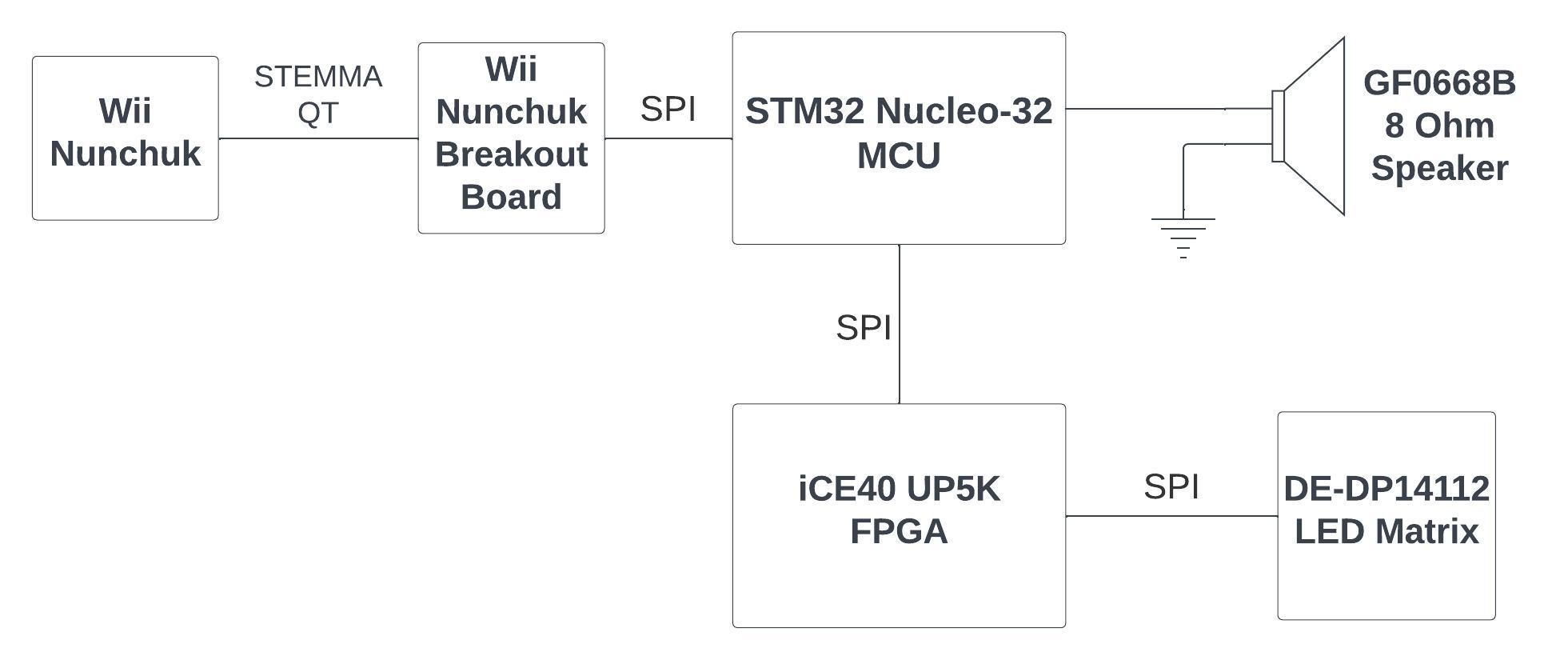
Fig 1. System-level block diagram, including the Wii Nunchuk, MCU, FPGA, LED Matrix, and speaker.
Once the Nunchuck message is received, it is parsed to pull out the x and y positions of the joystick and the states of the two buttons on the controller. Once these inputs are decoded, the MCU translates them into player movements and/or menu interactions and updates the game state as well as the screen that will be displayed on the LED Matrix. The display data is sent to the FPGA over SPI according to the communication standard defined in the FGPA design section. The MCU then waits for the DONE signal from the FPGA, signaling that the FPGA is done shifting data into the display and that the MCU can send over the next message.
FPGA Design
The LED matrix uses its own custom SPI-like communication protocol, shown in Figure 2. The matrix has four pins: CLK, CS, WR, and DATA. The DATA and WR pins act like the SDI and SCL pins from SPI, where data is written serially over DATA on the rising edge of WR to the matrix’s internal memory. The CLK and CS pins require a bit more explanation. The matrix contains four HT1632C LED driver chips, each of which controls a fourth of the display. Displaying an image on the matrix involves writing the proper bits to each of the four chips, and the CLK and CS pins allows one to select which chip to write to. CLK and CS are wired to the CP and DSA pins of a 74HC164 shift register, and the chip select pins of the four HT1632C chips are wired to the Q0, Q1, Q2, and Q3 pins.
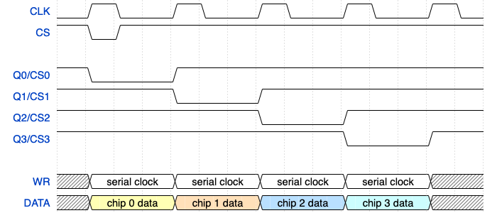
Fig 2. Timing diagram for the DE-DP14112 LED matrix.
The purpose of the FPGA is to receive a message over SPI from the MCU written using the communication standard defined earlier in this report, and to translate that SPI message into one following this custom protocol, which includes the proper bits, timing, and chip multiplexing. The digital circuit design, shown in Figure 4, follows the architecture of a processor, with a single controller managing the rest of the subcircuits through control signals. The state transition diagram for the controller is shown in Figure 3.
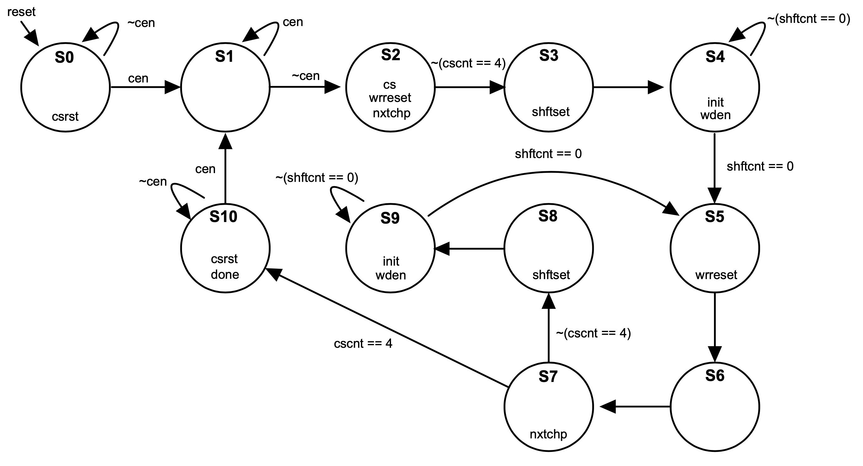
Fig 3. Finite state machine controller for the FPGA DE-DP14112 driver.
FPGA Block Diagram
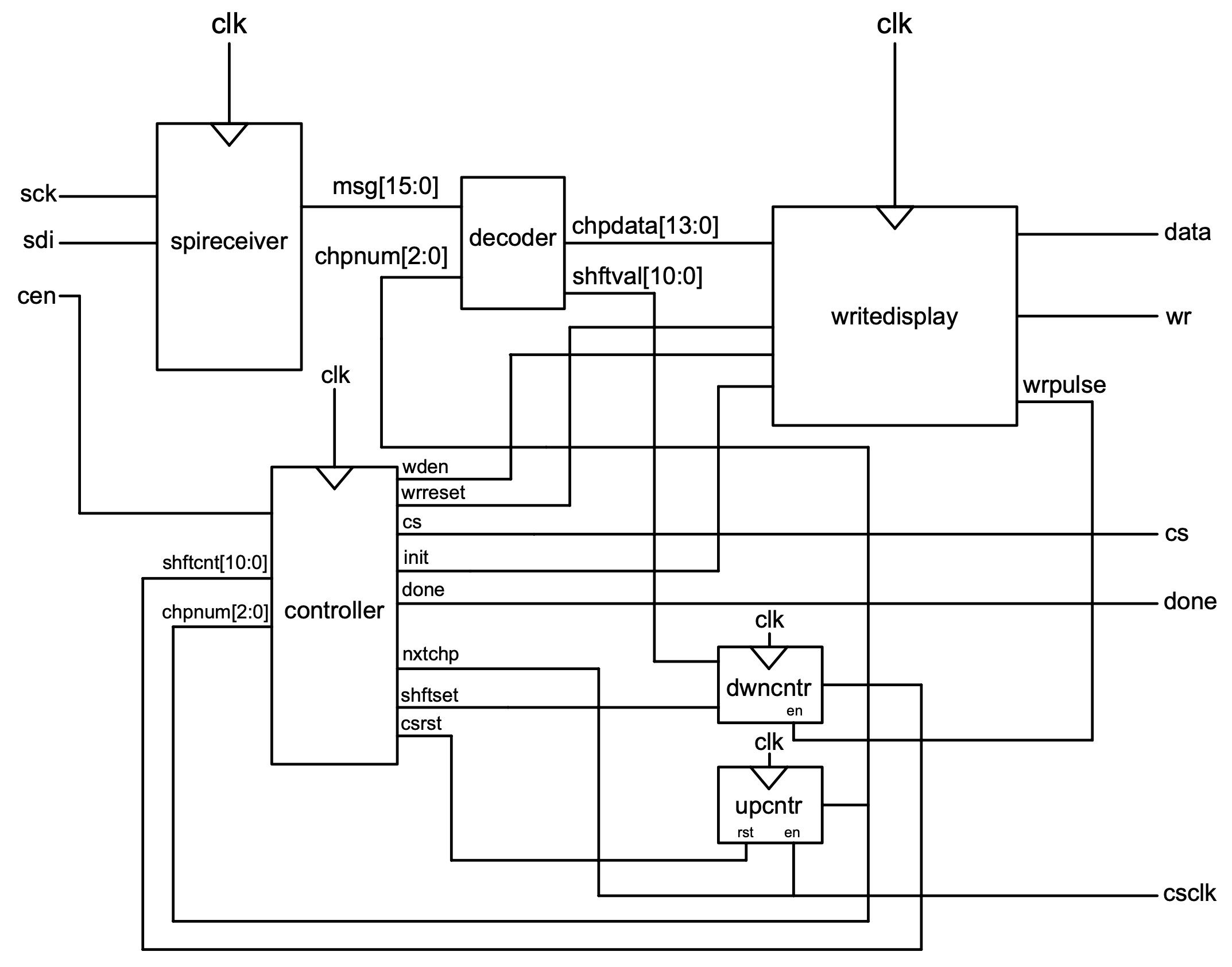
Fig 4. Block diagram for the FPGA DE-DP14112 driver.
MCU-to-FPGA Communication Standard
Communication between the MCU and FPGA occurs through 16-bit SPI transactions. The ID bit contains the operation type. The purpose of the remaining bits varies depending on whether the operation is a write or a command.
ID0 - B14 B13 B12 B11 B10 B9 B8 B7 B6 B5 B4 B3 B2 B1 B0
| ID | Instruction |
|---|---|
| 0 | Write |
| 1 | Command |
Table 1. Instructions corresponding to the ID bit
Write messages consist of position bits X[4:0] and Y[1:0], green LED control bits G[3:0], and red LED control bits R[3:0].
0 - R3 R2 R1 R0 - G3 G2 G1 G0 - Y1 Y0 - X4 X3 X2 X1 X0
As shown in Figure 5, the display is split into columns of four LEDs, where each LED in the column can be independently controlled. The write operation is used to control the LEDs in one of these columns, either by toggling them on/off, or by changing their color. The position bits X[4:0] and Y[1:0] define the (x, y) location of this column, defining (0, 0) to be at the top left of the display. The color bits R[3:0] and G[3:0] toggle the red and green LEDs respectively on each column.
X[4:0]: Control Location X
These bits are used to define the x-coordinate location of the column to be controlled, defining x = 0 as the left edge of the display.
Y[1:0]: Control Location Y
These bits are used to define the y-coordinate location of the column to be controlled, defining y = 0 as the top edge of the display.
G[3:0]: Green LED Enable
These bits individually toggle the four green LEDs within each column.
0: LED off
1: LED on
R[3:0]: Red LED Enable
These bits individually toggle the four red LEDs within each column.
0: LED off
1: LED on
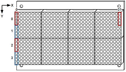
Figure 5. The display is split into columns of four LEDs. The four LEDs in a column can be controlled with a single write operation on that column.
The command operation is used to control system-level functionalities of the display. The command code bits CC[14:0] define the target functionality. Table 1 lists relevant command codes. Other command codes are listed in the HT1632C datasheet.
1 - CC14 CC13 CC12 CC11 CC10 CC9 CC8 CC7 CC6 CC5 CC4 CC3 CC2 CC1 CC0
| Name | CC[14:0] | Function |
|---|---|---|
| SYS DIS | 0000-0000-xxxxxxx | Turn off system oscillator |
| SYS EN | 0000-0001-xxxxxxx | Turn on system oscillator |
| LED Off | 0000-0010-xxxxxxx | Turn off LED duty cycle generator |
| LED On | 0000-0011-xxxxxxx | Turn on LED duty cycle generator |
Table 2. Command codes for toggling various system-level functionalities.