Digital Delay Pedal
UPDATE: This project has been indefinitely suspended due to being destroyed in a house fire (everyone was unharmed).
Summary
This ongoing project is my first practical venture into the field of digital signal processing. The goal is to design, build, and test a digital delay pedal with adjustable feedback and mix. I intend to use my ICE40UP5K FPGA from the arcade cabinet project as the digital audio processor, and separate ADC/DAC ICs to convert the audio signal to and from digital. Figure 1 shows a system-level block diagram of the planned design, where Km and Kf are the mix and feedback gains. Currently I have designed the digital delay unit at the register transfer level and verified its functionality using ModelSim. The next steps are to verify functionality in hardware, then start on the analog signal processing circuitry.
Problem Statement
Building the delay pedal involves designing and integrating multiple sub-systems, including any analog signal conditioning circuitry at the audio input and output, the ADC and DAC, and the digital delay unit itself. Figure 1 shows how I plan to connect these subsystems. I predict the brunt of the design work to be in the digital delay unit, as I must not only implement the digital delay, but also interface the delay unit with the 12-bit ADC and DAC ICs, both of which use SPI to send/receive digital audio data. I must continually reference the ADC and DAC datasheets to ensure that my delay unit complies with the manufacturer’s timing specifications. The next challenge is to design the single-supply op-amp circuitry for conditioning the analog signal, which will involve some combination of biasing circuitry, virtual grounding, and AC coupling capacitors to shift the signal center point as needed.
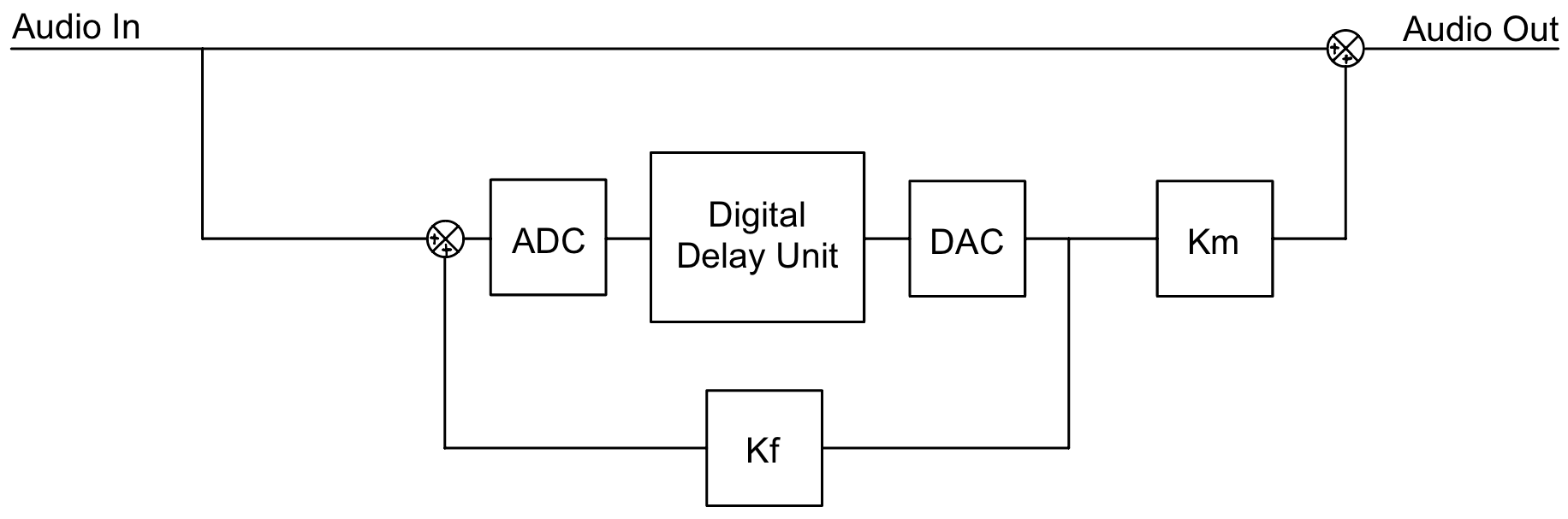
Fig 1. System-level block diagram for an FPGA-based digital delay pedal.
Digital Delay Unit
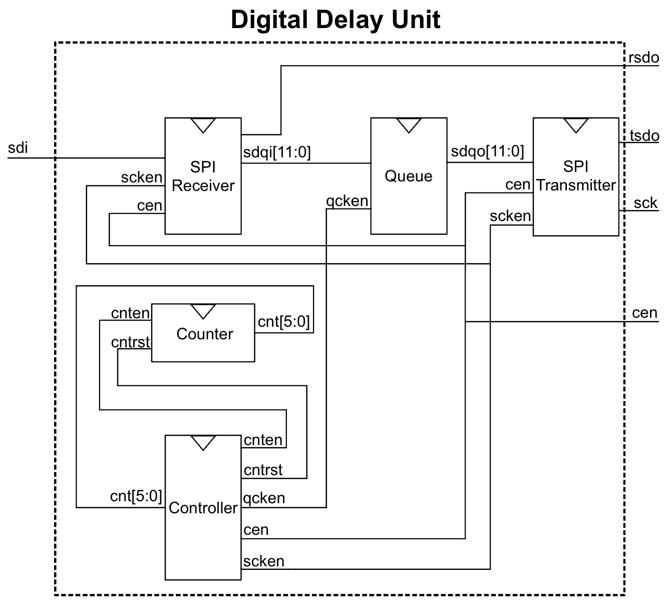
Fig 2. Block diagram of the digital delay unit at the register transfer level
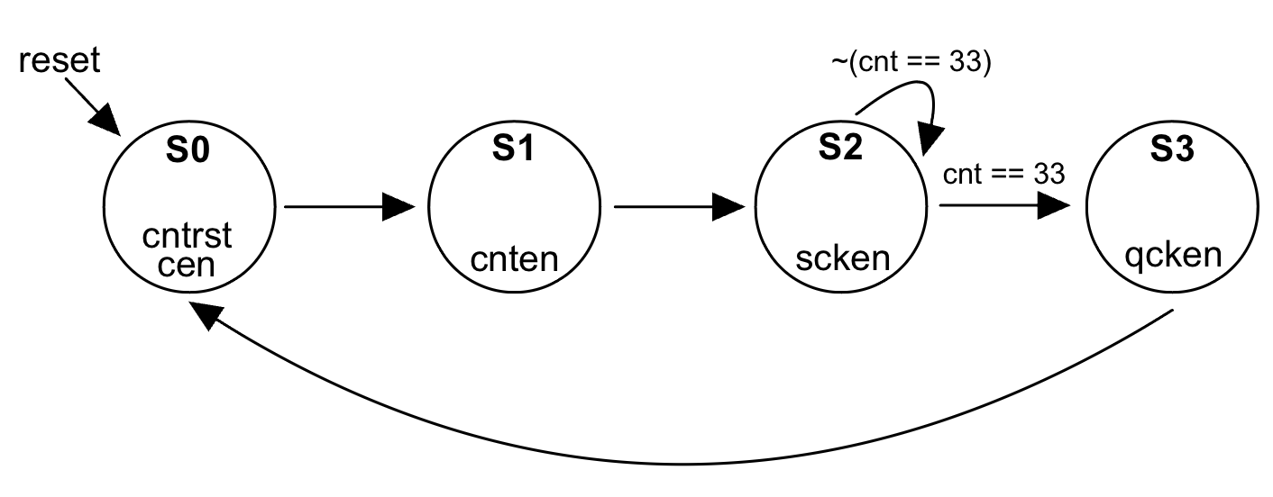
Fig 3. Finite state machine showing the high-level behavior of the digital delay unit.
Updates on the first physical prototype coming as soon as I finish the documentation