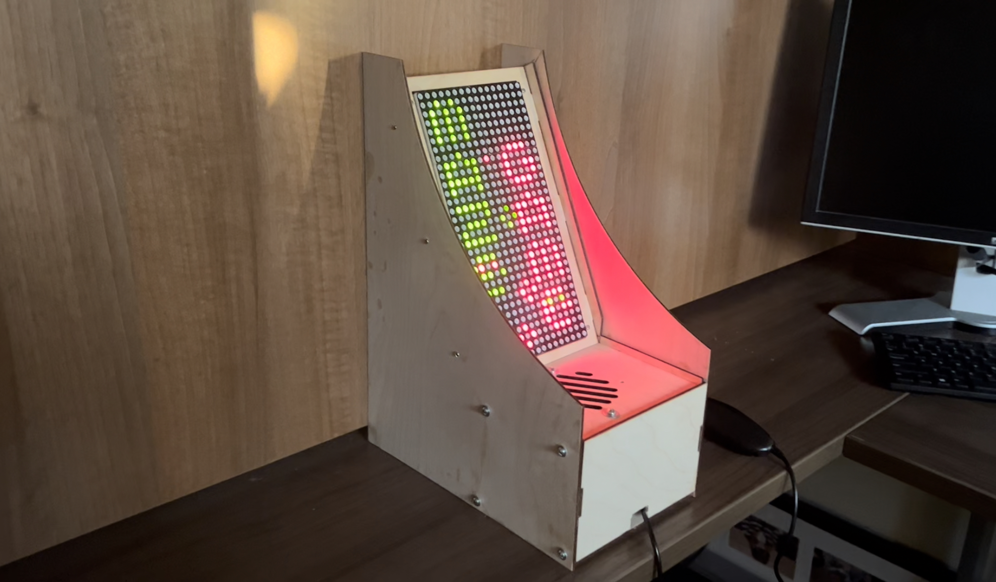
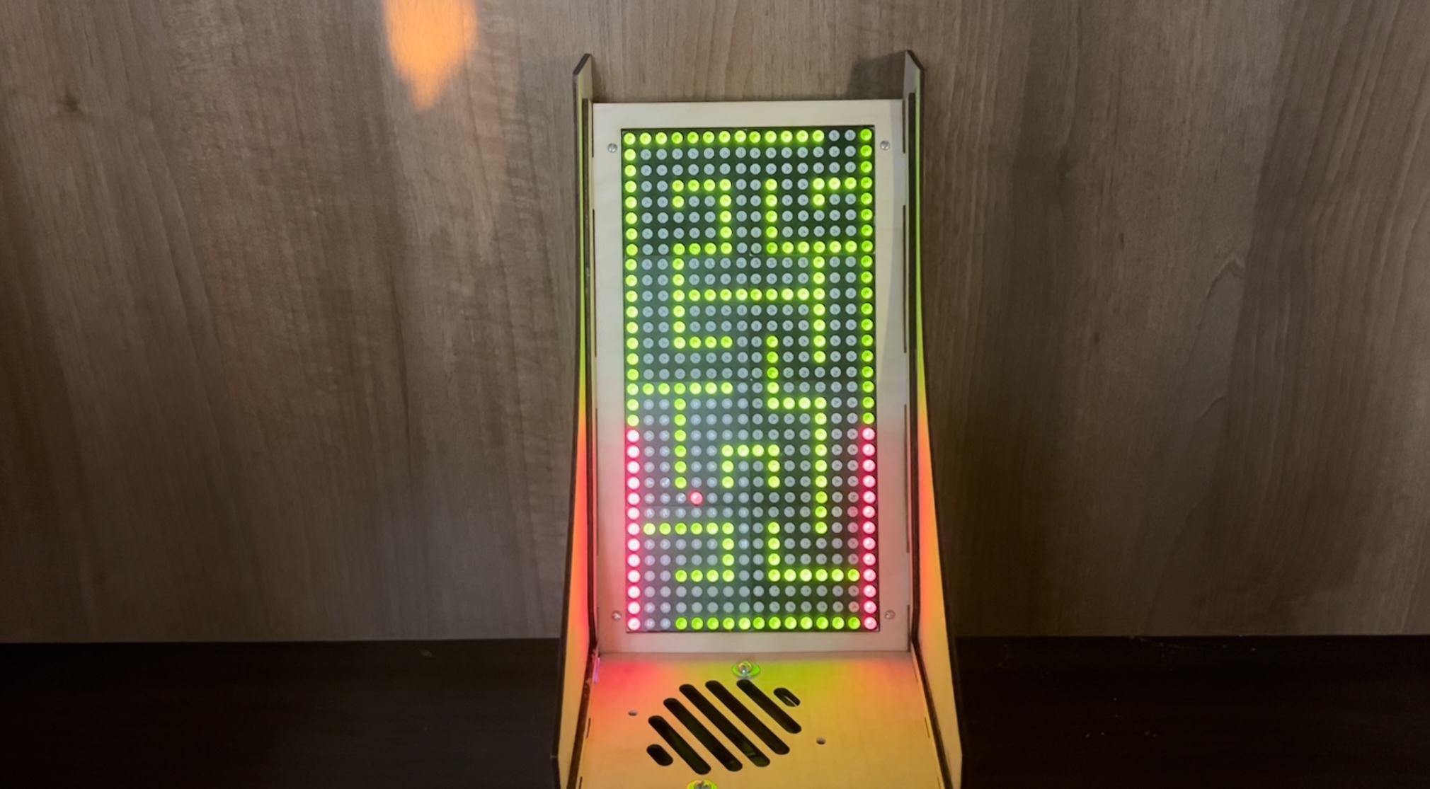
Model Arcade Cabinet
Demo Video

Summary
As part of an embedded systems course, I and two of my friends constructed a 1/5 scale arcade cabinet using an STM32L432KC microcontroller and an ICE40UP5K FPGA. As shown in Figure 1, the project involved integrating together five digital systems: an MCU, FPGA, LED matrix, speaker, and Wii Nunchuk controller. I was solely responsible for interfacing the FPGA, LED matrix, and speaker with the MCU, so I will mostly speak to that part of the project. Shoutout to my friends Lawrence and Cecilia for their great work on the I2C controller communication and mechanical design of the cabinet.
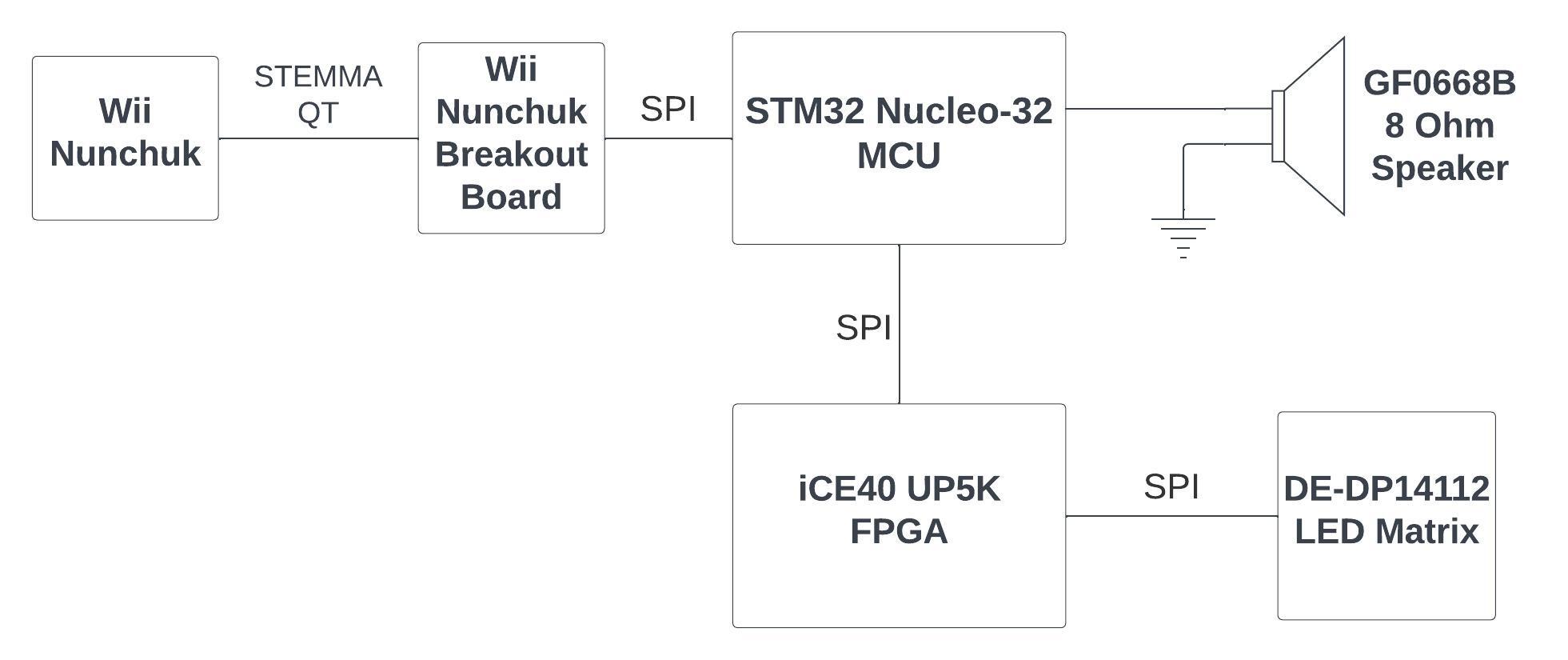
Fig 1. System-level block diagram, including the Wii Nunchuk, MCU, FPGA, LED Matrix, and speaker.
Problem Statement
The LED matrix uses its own custom SPI-like communication protocol, shown in Figure 2. The matrix has four pins: CLK, CS, WR, and DATA. The DATA and WR pins act like the SDI and SCL pins from SPI, where data is written serially over DATA on the rising edge of WR to the matrix’s internal memory. The CLK and CS pins require a bit more explanation. The matrix contains four HT1632C LED driver chips, each of which controls a fourth of the display. Displaying an image on the matrix involves writing the proper bits to each of the four chips, and the CLK and CS pins allows one to select which chip to write to. CLK and CS are wired to the CP and DSA pins of a 74HC164 shift register, and the chip select pins of the four HT1632C chips are wired to the Q0, Q1, Q2, and Q3 pins.
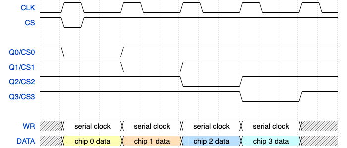
Fig 2. Timing diagram for the DE-DP14112 LED matrix.
So why the FPGA?
The purpose of the FPGA is to receive a message over SPI from the MCU, and to translate that SPI message into one following this custom protocol. One alternative to using the FPGA would be to bit-bang this custom protocol on the MCU, but that would likely limit the functionalities I could include in the arcade game since the processor would spend most of its time and energy just sending messages to the FPGA. To allow me to take full advantage of the MCU’s hardware SPI peripheral, I designed a digital circuit at the register transfer level (RTL) shown in Figure 4, which uses the architecture where a single controller manages the rest of the subcircuits through control signals. The state transition diagram for the controller is shown in Figure 3. I then programmed my ICE40UP5K FPGA to run this circuit using SystemVerilog. I should note that if my intention was to produce many of these cabinets at low cost, I would instead search for a way to hack together the available peripherals on the STM32 rather than purchase a whole FPGA just to avoid bit-banging. I only plan to make one of these, and I have been seeking opportunities to improve my FPGA development skills, so FPGA it was.
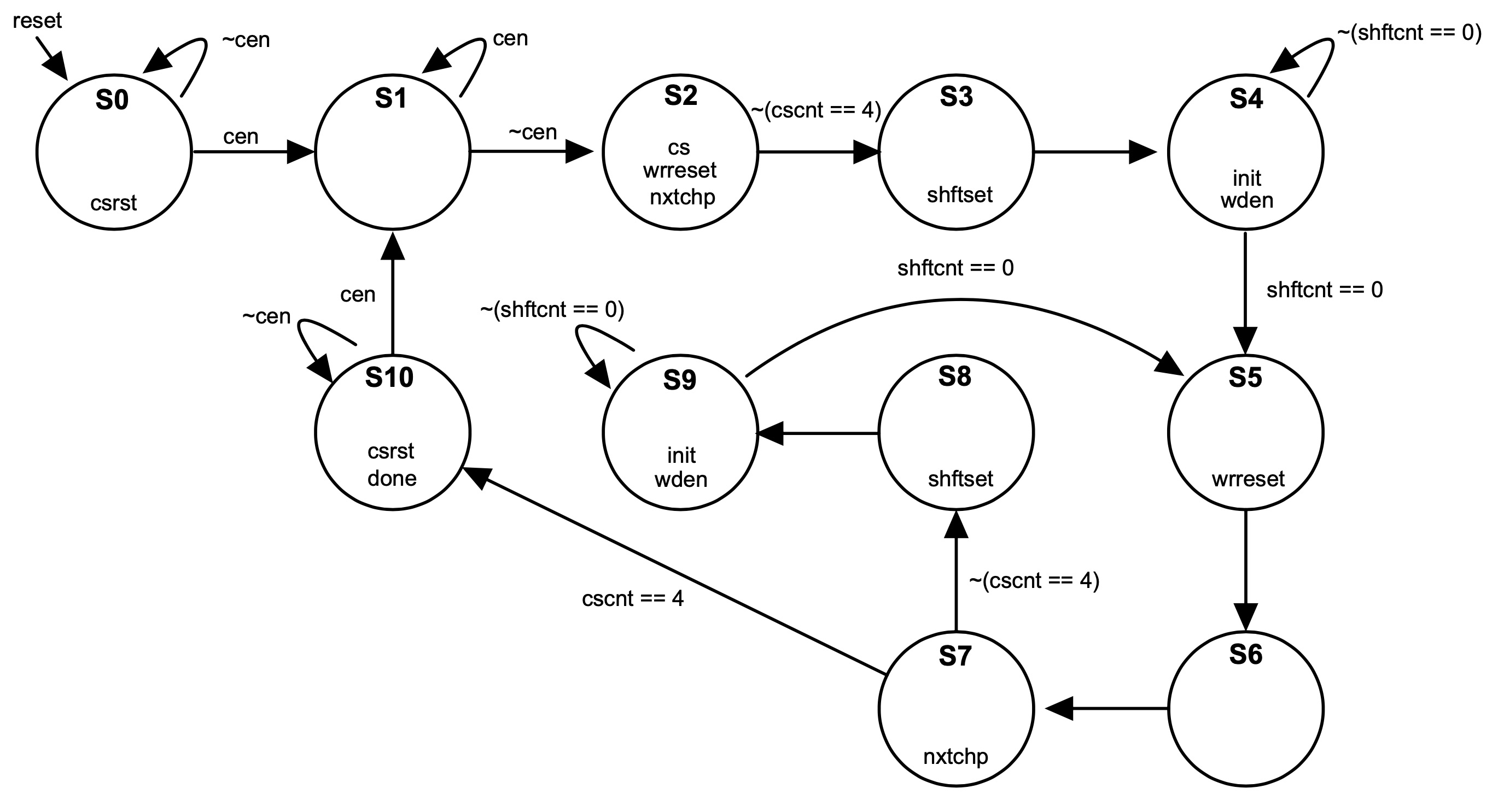
Fig 3. Finite state machine controller for the FPGA DE-DP14112 driver.
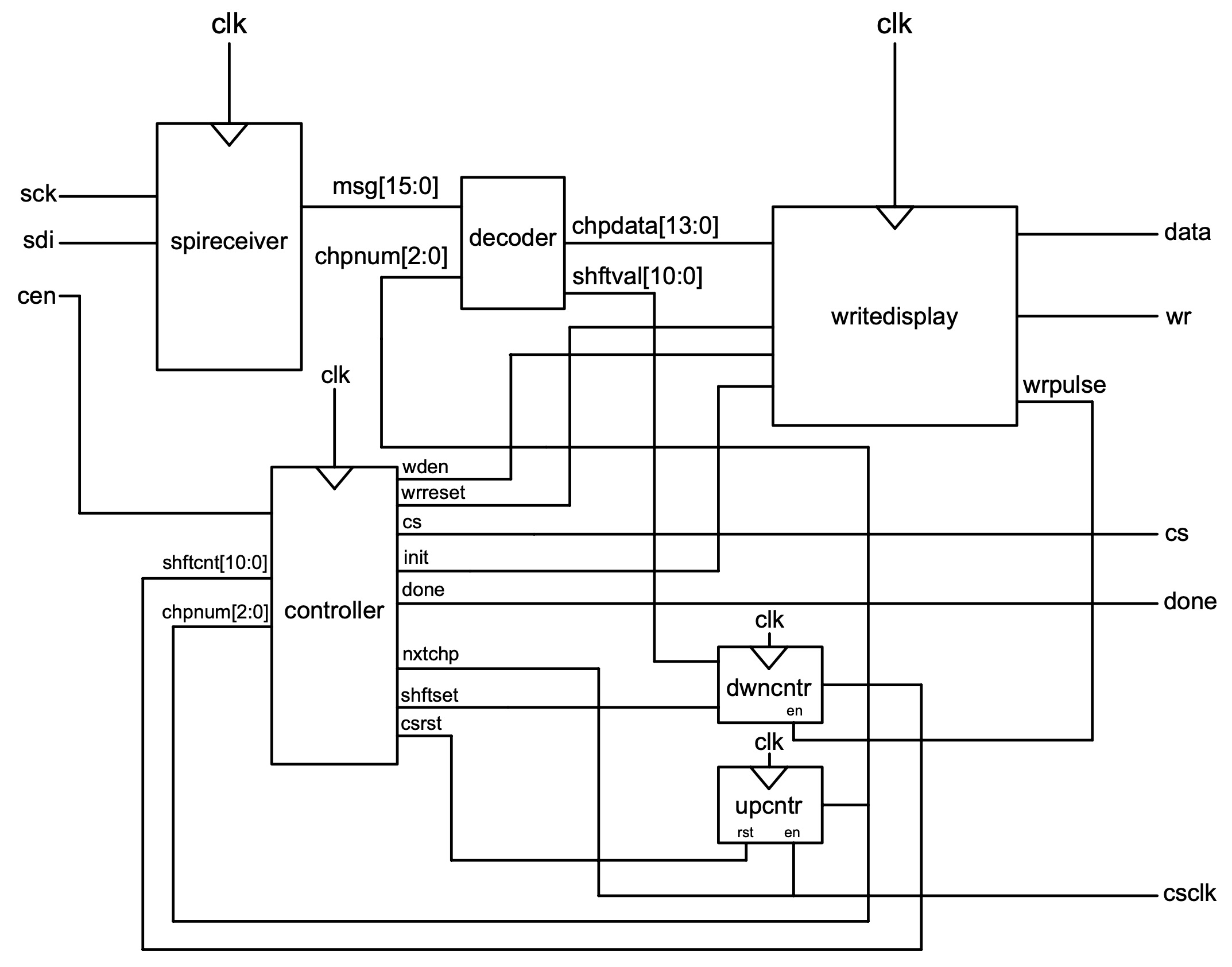
Fig 4. Block diagram for the FPGA DE-DP14112 driver.
MCU-to-FPGA Communication Standard
The MCU controls the LED display by sending messages to the FPGA over SPI. I defined the following 16-bit message format for MCU-FPGA communication. Each message starts with an ID bit which contains the operation type. The purpose of the remaining bits varies depending on whether the operation is a write or a configuration command.
ID0 - B14 B13 B12 B11 B10 B9 B8 B7 B6 B5 B4 B3 B2 B1 B0
| ID | Instruction |
|---|---|
| 0 | Write |
| 1 | Command |
Table 1. Instructions corresponding to the ID bit
Write messages consist of position bits X[4:0] and Y[1:0], green LED control bits G[3:0], and red LED control bits R[3:0].
0 - R3 R2 R1 R0 - G3 G2 G1 G0 - Y1 Y0 - X4 X3 X2 X1 X0
As shown in Figure 5, the display is split into columns of four LEDs, where each LED in the column can be independently controlled. The write operation is used to control the LEDs in one of these columns, either by toggling them on/off or by changing their color. The position bits X[4:0] and Y[1:0] define the (x, y) location of this column, defining (0, 0) to be at the top left of the display. The color bits R[3:0] and G[3:0] toggle the red and green LEDs respectively on each column. You might be wondering why I mandate that a single message must control four LEDs at once. The reason for this is in the way that the HT1632C LED matrix driver chips are structured. Each chip contains a display memory consisting of multiple registers and each register contains four bits, each of which corresponds to one LED in a column of four. A write operation may only write starting from bit zero of a given register.
X[4:0]: Control Location X
These bits are used to define the x-coordinate location of the column to be controlled, defining x = 0 as the left edge of the display.
Y[1:0]: Control Location Y
These bits are used to define the y-coordinate location of the column to be controlled, defining y = 0 as the top edge of the display.
G[3:0]: Green LED Enable
These bits individually toggle the four green LEDs within each column.
0: LED off
1: LED on
R[3:0]: Red LED Enable
These bits individually toggle the four red LEDs within each column.
0: LED off
1: LED on
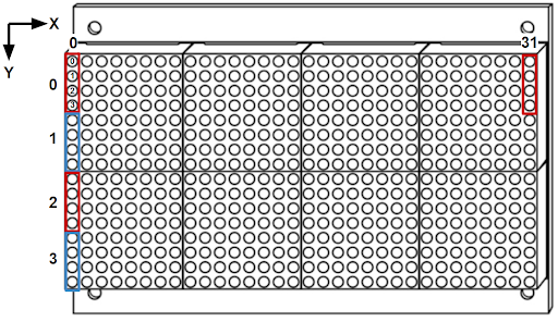
Figure 5. The display is split into columns of four LEDs. The four LEDs in a column can be controlled with a single write operation on that column.
The command operation is used to control system-level functionalities of the display. The command code bits CC[14:0] define the target functionality. Table 1 lists relevant command codes. Other command codes are listed in the HT1632C datasheet.
1 - CC14 CC13 CC12 CC11 CC10 CC9 CC8 CC7 CC6 CC5 CC4 CC3 CC2 CC1 CC0
| Name | CC[14:0] | Function |
|---|---|---|
| SYS DIS | 0000-0000-xxxxxxx | Turn off system oscillator |
| SYS EN | 0000-0001-xxxxxxx | Turn on system oscillator |
| LED Off | 0000-0010-xxxxxxx | Turn off LED duty cycle generator |
| LED On | 0000-0011-xxxxxxx | Turn on LED duty cycle generator |
Table 2. Command codes for toggling various system-level functionalities.
Pictures